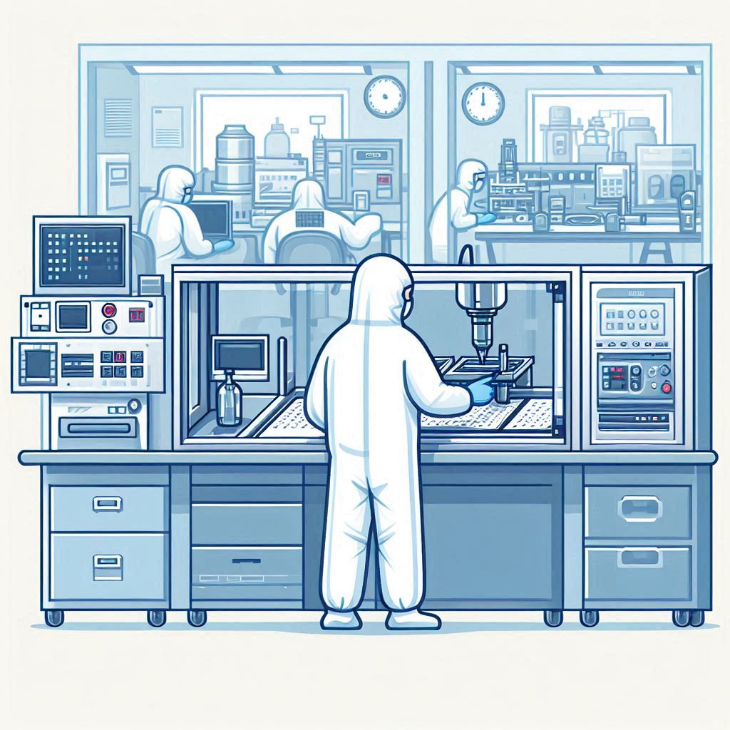
This activity will allow participants to experience entering a clean room and learn how to correctly put on and take off clean clothes, shoes, hair caps, masks, gloves and other equipment to ensure operation in a highly clean environment. Then, you can simply participate in the coating and exposure lithography technology in the semiconductor manufacturing process. Coating is to evenly cover the wafer surface with a thin film, while exposure lithography technology uses photolithography technology to create fine patterns. Finally, it also allows participants to understand the applications and characteristics of components in electronics, biomedicine, materials and other fields. This experience allows participants to have a more intuitive understanding of high-tech manufacturing processes.
Activity Information
 Speaker
Dr. Shu-Yi Hsieh
 Time
Time
10/19 09:00 - 16:00
 Location
Interdisciplinary Research Building for Science and Technology
Venue
1F Lobby
Activity Classification
 Division
Division of Mathematics and Physical Sciences
 Category
Interactive Experience
Organizer
Target Audience
Age 12 and above
Instructions
Contact
CHOU, Chia-I
2787-3103
 Note
Note
On-Site Registration is required.